Step by step from ordering to the first sound: Tonwerk Wavetable as a Eurorack module on the through-hole boards (v0.1), everything to solder yourself; only the ESP32 DevKit and the DAC module come ready-made and are plugged in.
If you would rather not solder that much: the main board also comes as an assembled SMD variant that the board manufacturer delivers soldered.
Important for the v0.1 boards: the silkscreen of the two LEDs is the wrong way round. Inserted as printed, +5 V and ground reach the LED swapped, and it burns out the first time it is powered. The right orientation is in step 5.
As of 28 October 2026: one module has been built following this guide and plays (27 October 2026). Not yet tested on the hardware: the CV inputs and the V/Oct calibration. If you build one, feedback on GitHub helps improve the guide and the boards. File names and the boards' labels are German: Hauptplatine is the main board, Bedienplatine the control board, Frontplatte the front panel, Knopf a knob.
Soldering iron with a fine tip, solder, side cutters, multimeter.
A Eurorack case with ±12 V; for the first power-up, better a bench supply with current limiting.
A computer with Chrome or Edge (for flashing in the browser) and a USB cable that carries data.
A 3D printer for the front panel and knobs (or 2 mm aluminium and a drill for the front).
For calibration, a voltage source for exactly 1.000 V and 3.000 V (a bench supply and the multimeter will do).
1. Ordering
Boards: upload the two Gerber zips (Downloads) to a board manufacturer, JLCPCB for example: 5 of each, 2 layers, 1.6 mm, HASL, without assembly. Leave the other settings as the manufacturer suggests. Both boards are 66 × 107.5 mm.
Parts: the shopping list below, an estimated €60–80 plus boards. DevKit, DAC module, pots, jacks and LEDs are cheapest from the large Chinese shippers, the chips, resistors and capacitors from any electronics distributor.
What matters:
ESP32-S3-DevKitC-1 N16R8: N16R8 means 16 MB flash and 8 MB PSRAM. Without the 8 MB of PSRAM the firmware does not run; the tables need 5.7 MB. Clones work if the pinout is the same.
PCM5102A module “GY-PCM5102” (purple) with the 6-pin header VIN GND LCK DIN BCK SCK.
74HCT125 or 74AHCT125, not 74HC125: that one does not reliably read the ESP32's 3.3 V at 5 V. A 74HCT32 fits the same holes without changes.
WS2812D-F5 (5 mm, through-hole) with the pins 1 DIN, 2 VDD, 3 GND, 4 DOUT; check the seller's datasheet. The flat side is at DOUT. APA106s are often sold under this name (as on the first module): same pin order, but red-green-blue instead of green-red-blue. The ready-made images are made for those; genuine Worldsemi WS2812D-F5s need their own firmware build (see troubleshooting).
Electrolytic capacitors at most 11 mm tall, 2 mm pitch.
Pots 9 mm vertical, B10K linear. Their shaft sticks out only a little behind the printed front; the knobs to print are made for that.
Shopping list
Qty
Part
Type
Where
approx. €
1
Boards
tonwerk-bedien-tht + tonwerk-haupt-tht, 5 of each, 2 layers, 1.6 mm, HASL, unassembled
—
15–30 with shipping
1
Microcontroller board
ESP32-S3-DevKitC-1 N16R8 (16 MB flash, 8 MB PSRAM), original or clone with the same pinout
74HCT125 or 74AHCT125 (DIP-14), not 74HC125; equivalent without changing the board: 74HCT32 (DIP-14)
Main U10
0.40
1
Voltage regulator 3.0 V
MCP1700-3002E/TO (TO-92)
Main U3
0.50
1
Transistor
BC547 (TO-92)
Main Q1
0.10
1
Switching regulator
Recom R-78E5.0-0.5 (SIP-3)
Main U1
3.00
3
Schottky diode
1N5817 (DO-41)
Main D1-D3
0.20
4
IC socket
3 × DIP-14, 1 × DIP-16 (plus 1 × DIP-8, see next row)
Main
0.60
1
IC socket
DIP-8
Main
0.10
10
Resistor 1 %
100k (metal film 0207, 1/4 W)
Main
0.80
7
Resistor 1 %
1k
Main
0.60
5
Resistor 1 %
10k
Main
0.40
4
Resistor 1 %
30k
Main
0.30
2
Resistor 1 %
6.8k
Main
0.20
1
Resistor 1 %
37.4k
Main
0.10
1
Resistor 1 %
17.4k
Main
0.10
1
Resistor 1 %
16k
Main
0.10
1
Resistor 1 %
330 Ω
Main
0.10
1
Resistor 1 %
10 Ω
Main
0.10
20
Ceramic capacitor
100 nF X7R, 2.54 mm pitch (18 main, 2 control)
both
1.20
5
Ceramic capacitor
10 nF, 2.54 mm pitch
Main
0.30
2
Ceramic capacitor
1 µF X7R, 2.54 mm pitch
Main
0.30
4
Electrolytic capacitor
10 µF 25 V radial, 5 mm diameter, at most 11 mm tall, 2 mm pitch
Main
0.40
2
Female header
1 × 22, 2.54 mm pitch, 8.5 mm tall (or cut 2 × 1 × 40 down)
Main (DevKit)
1.50
1
Female header
1 × 6, 2.54 mm pitch, 8.5 mm tall
Main (DAC module)
0.30
2
Female header
1 × 14, 2.54 mm pitch, 8.5 mm tall
Main J3 J4
0.80
2
Pin header
1 × 14, 2.54 mm pitch, straight
Control J3 J4
0.30
1
Boxed header
2 × 5, 2.54 mm pitch, straight
Main J1
0.30
—
Hook-up wire
3 short wires from the DAC module's output (L, ground, R) to J13
Main
—
10
Potentiometer
Alpha 9 mm vertical, B10K linear (footprint Alpha RD901F), shaft to match the knobs
Control
3–6
10
Knob
the knobs to print (above), otherwise to match the shaft, at most 13 mm diameter
—
—
8
Jack socket
PJ398SM (Thonkiconn or clone)
Control
2–4
2
Push button
6 × 6 mm, 13 mm tall
Control
0.50
2
RGB LED
WS2812D-F5, 5 mm through-hole (check the pinout 1 DIN, 2 VDD, 3 GND, 4 DOUT)
Control
1–2
1
Eurorack cable
ribbon cable 10 to 16 pin
—
1–2
2
Standoffs
M3 × 11 mm female/female + 4 screws M3 × 5
—
1.00
4
Rack screws
M3 × 6 with nylon washers
—
0.50
1
Front panel
print frontplatte.stl (above)
—
1.00
2. Printing the front panel and knobs
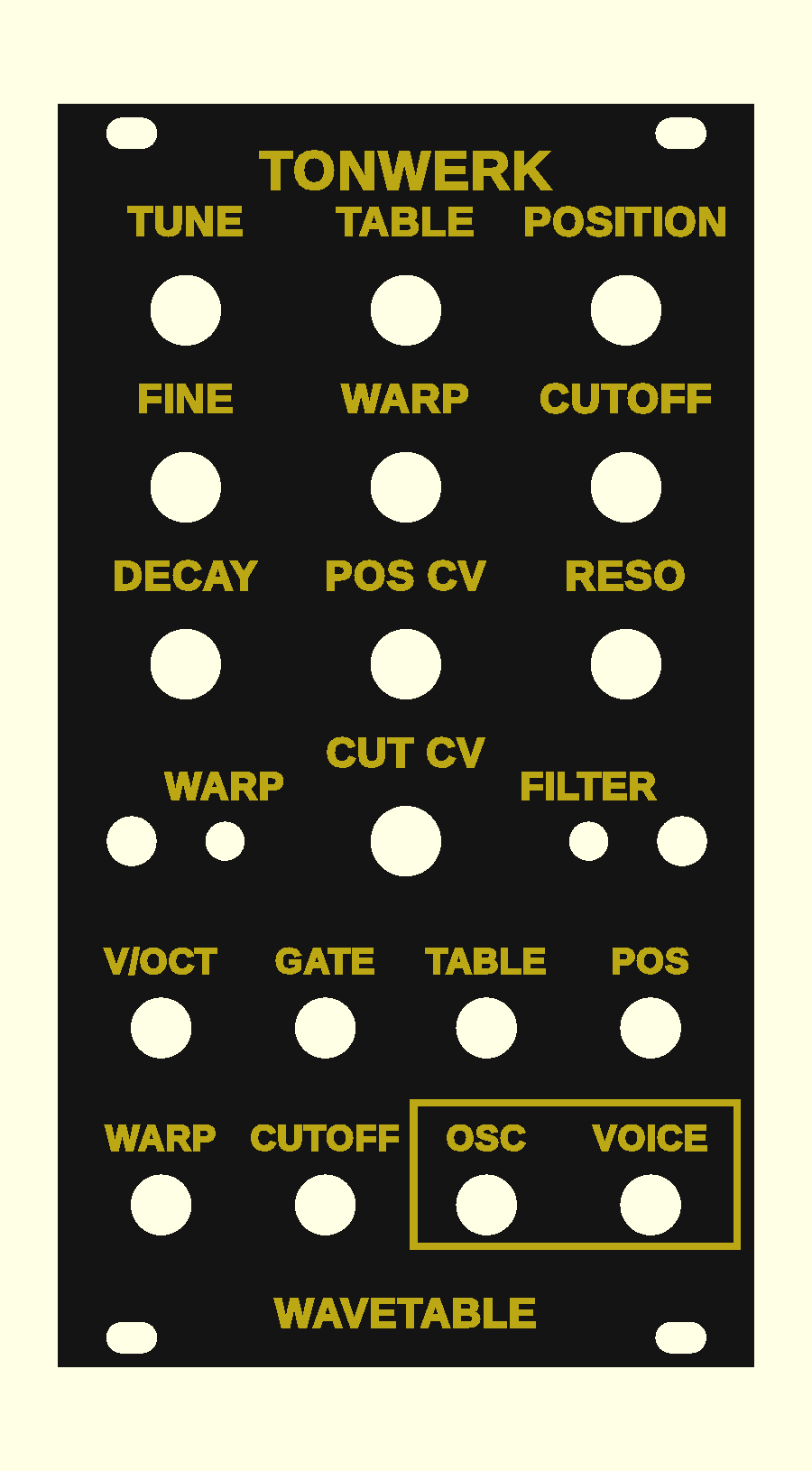
14 HP (70.8 × 128.5 mm), 2.5 mm thick, with slots for the rack screws. Three variants, all already oriented for printing (PETG or PLA, 0.2 mm layers):
Raised lettering (frontplatte.stl): print with the front facing up, change filament at 2.5 mm height (after layer 13). The simplest; the module above is printed this way.
Engraved lettering (frontplatte-graviert.stl): front facing up, fill the lettering with acrylic paint or wax and wipe the front clean.
Inlaid lettering (frontplatte-einlage.3mf): for printers with several colours or a tool changer, front facing down; assign a tool to each of the two parts “Platte” (plate) and “Schrift” (lettering). The lettering is as deep as the first layer (0.5 mm).
For the Physical firmware there are the same three variants with its lettering (frontplatte-physical*.stl, frontplatte-physical-einlage.3mf, Downloads), meant to be yellow with black lettering: for the raised print start with yellow and change to black at 2.5 mm. The same for the PD, the Granular and the Additiv firmware (frontplatte-pd*, frontplatte-granular*, frontplatte-additiv*), in colours of your choice; Granular is meant to be magenta with black lettering, for the raised print start with magenta and change to black at 2.5 mm.
Hole sizes: pots 7.2 mm, jacks 6.2 mm, LEDs 5.1 mm, buttons 4.0 mm. After printing, push a pot, a jack, an LED and a button through once: the front is the jig when soldering the control board.
Knobs
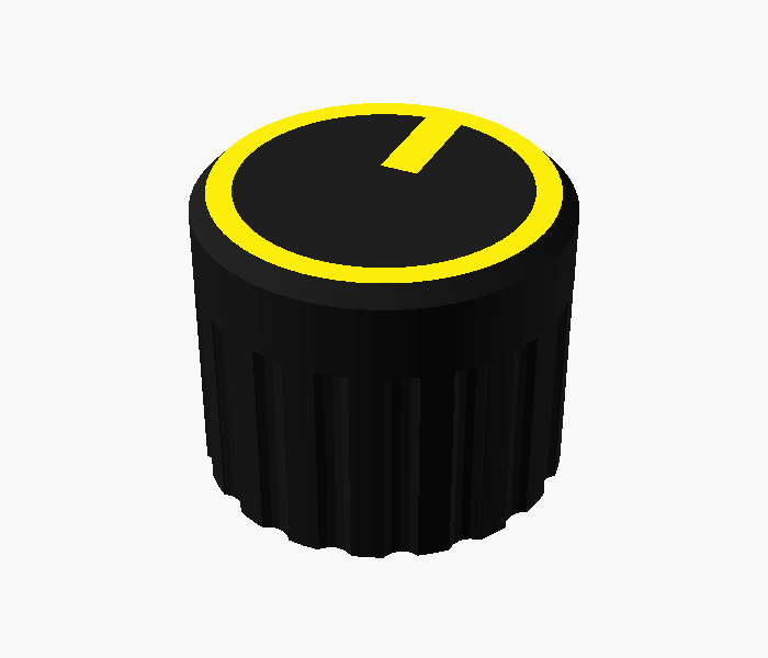
Black with a yellow pointer and ring, 13.4 mm in diameter. Underneath, the knob has a recess over the nut and washer, so it sits firmly even on the short shaft and almost on the front.
The knobs have a bore of 6.15 mm: on the first build, 5.9 and 6.0 mm were too tight and 6.1 mm a little too snug, as printed holes come out smaller. On another printer, print the fit test first: three rings with bores of 6.05, 6.15 and 6.25 mm (one, two, three marks). Push them onto a shaft; if another than the middle one fits snugly, enter its size as shaft_d in knopf.scad and export again. Also there: D shaft instead of knurled, shaft length, nut height.
Then knopf.3mf: ten knobs, each with the parts “Körper” (body) and “Zeiger” (pointer). They are printed cap down; the pointer is the first layer, so it has the same smooth surface as the rest.
With only one nozzle: the first layer yellow, then change to black. The whole cap is then yellow; if you do not want that, set einlage = false in the .scad.
3. Soldering the main board
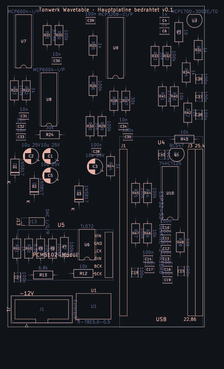
Everything goes on the back (the side with the silkscreen, which faces backwards in the module), only the two 14-pin female headers J3 and J4 on the front. Under the DevKit and the DAC module there is room only for flat parts, so go from flat to tall:
Silkscreen of the main board, seen from the back. Tap to enlarge.
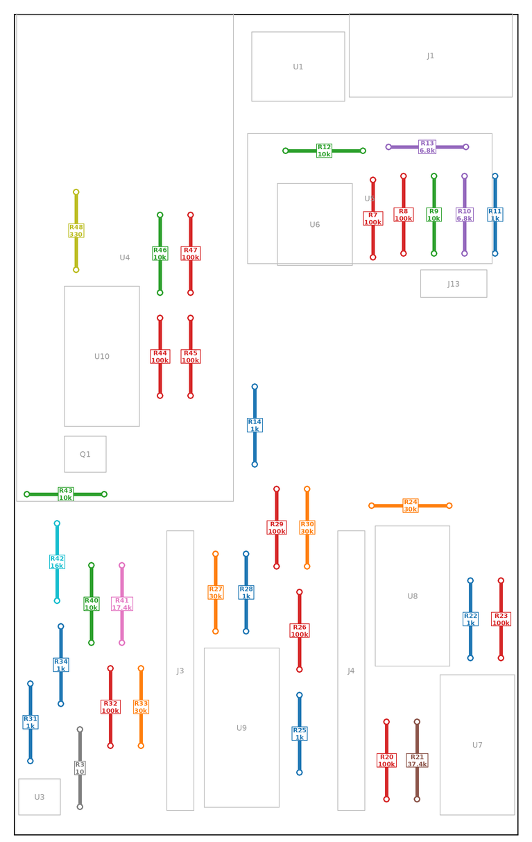
Resistors. Measure each with the multimeter before soldering: the colour bands of 1 % resistors are easy to mix up.
Value
Parts
10 Ω
R3
330 Ω
R48
1k
R11 R14 R22 R25 R28 R31 R34
6.8k
R10 R13
10k
R9 R12 R40 R43 R46
16k
R42
17.4k
R41
30k
R24 R27 R30 R33
37.4k
R21
100k
R7 R8 R20 R23 R26 R29 R32 R44 R45 R47
The resistors coloured by value, component side, boxed header at the top right.
Diodes 1N5817: D1, D2, D3. The band marks the cathode, as on the silkscreen.
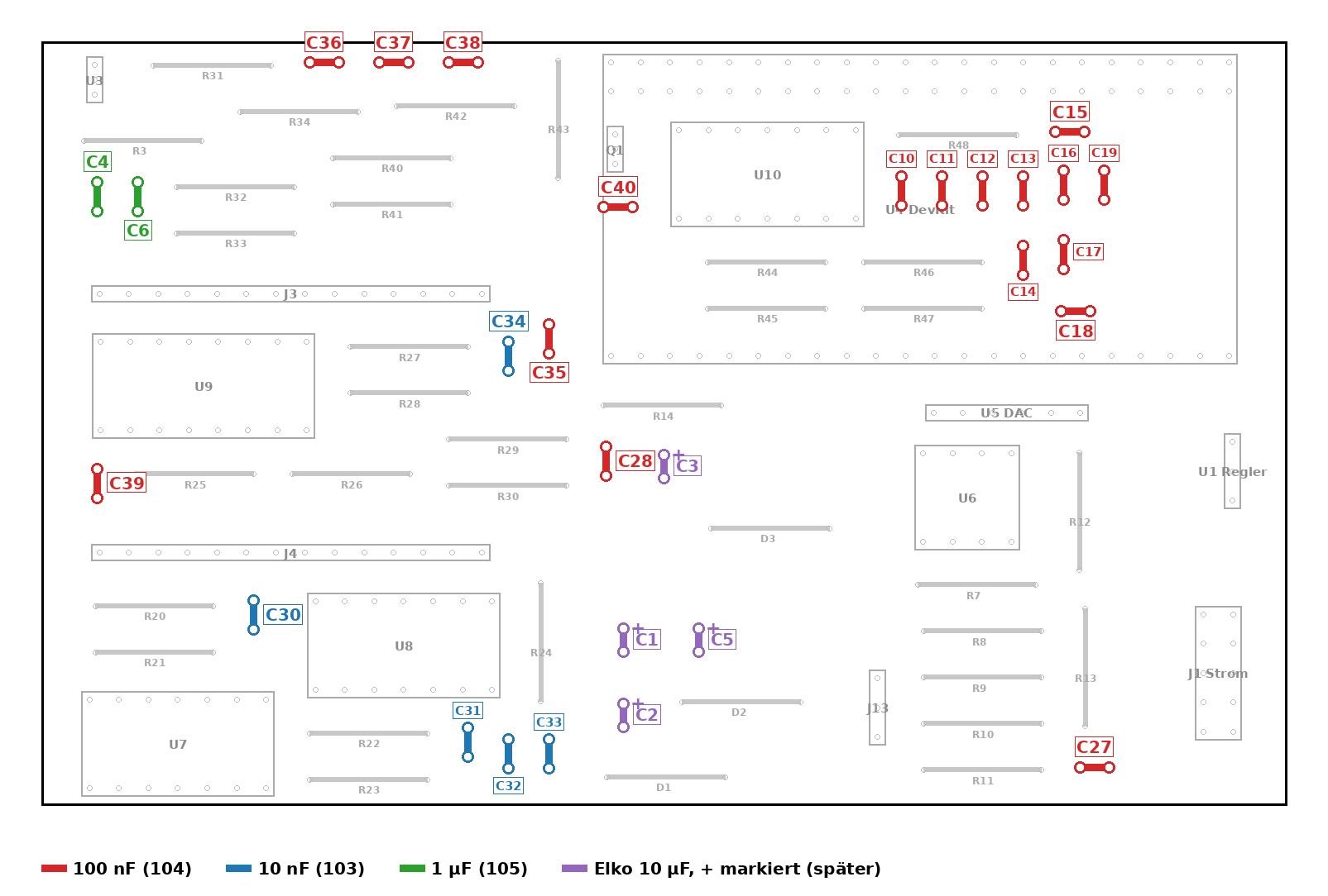
Ceramic capacitors: 100 nF (C10–C19, C27, C28, C35–C40), 10 nF (C30–C34), 1 µF (C4, C6). They have no polarity.
The capacitors coloured by value, board turned sideways (boxed header at the bottom right). The electrolytics (purple) come only in step 8.
IC sockets: DIP-8 (U6), DIP-14 (U7, U8, U10), DIP-16 (U9). The notch as on the silkscreen. The chips go in only in step 7.
TO-92: Q1 BC547 (flat side as on the silkscreen) and U3 MCP1700-3002E (3.0 V reference; pin 1 GND, 2 IN, 3 OUT, check the datasheet before soldering).
J13: three pins (L, ground, R) for the wires from the DAC module, straight from the component side.
Female headers for the modules: two 1 × 22 for the DevKit, one 1 × 6 for the DAC module, all 8.5 mm tall. First measure the distance between the two pin rows on your own DevKit: the original has 25.4 mm, some clones 22.86 mm; for the narrower one J3 has a second row of holes further in (labelled “22,86”). Best plug the DevKit into the headers, insert them like that and then solder, so they stand straight.
Electrolytic capacitors 10 µF: C1, C2, C3, C5. Mind the polarity: C1 + to +12 V, C2 + to ground (it sits on −12 V), C3 + to +5 V, C5 + to +3V3A.
Switching regulator U1 (R-78E5.0-0.5), label as on the silkscreen.
Boxed header J1 (Eurorack power): pin 1 is −12 V, where the cable's red stripe goes.
Last, on the front, the female headers J3 and J4 (1 × 14, pin 1 at the top). So that they match the control board: plug in the control board's pin headers, screw both boards together with the standoffs (M3 × 11 mm) and only then solder. This can also wait until after step 5.
4. Preparing the DAC module
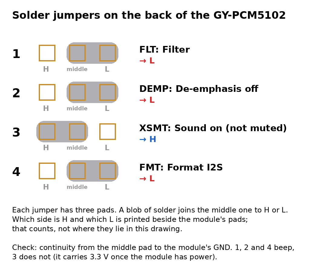
On the back of the GY-PCM5102 there are four solder jumpers with three pads each. With a blob of solder connect the middle pad to L (ground) or H:
Jumper
Function
Setting
1 FLT
Filter
L
2 DEMP
De-emphasis
L (off)
3 XSMT
Soft mute
H (sound on)
4 FMT
Data format
L (I2S)
The blob of solder joins the middle pad to H or L. Which side is H is printed as a letter on the module; the layout may differ from the drawing.
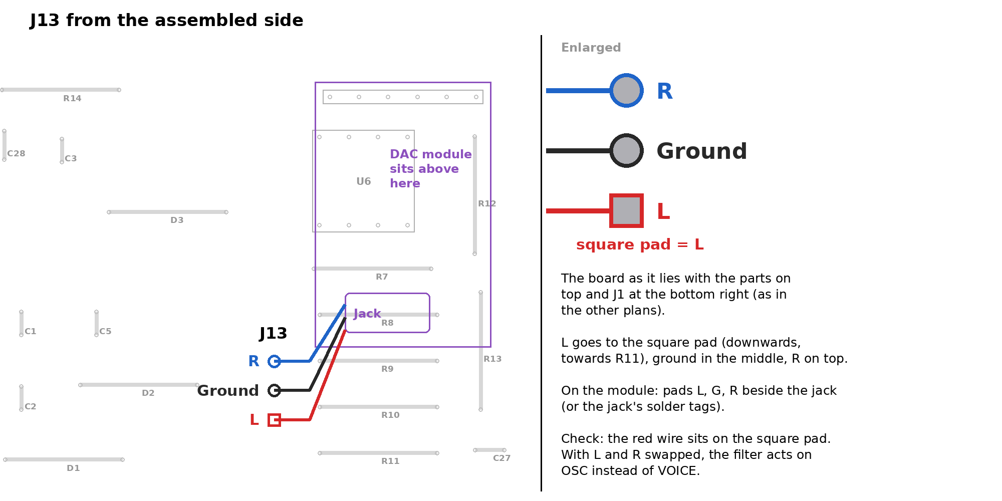
Some modules come set this way already or without jumpers at all. SCK needs no wire, the board ties it to ground. Solder the pin header so that the module's labels match those on the main board (VIN GND LCK DIN BCK SCK). Then three short wires from the pads L, G, R next to the module's jack (or its solder lugs) to J13: L, ground, R. L is at J13's square pad, ground is the middle pin. With L and R swapped, the filter acts on the OSC output instead of VOICE.
Three wires from the module to J13, seen from the component side, J1 at the bottom right as in the other plans. On the right J13 enlarged: L belongs on the square pad.
5. Soldering the control board
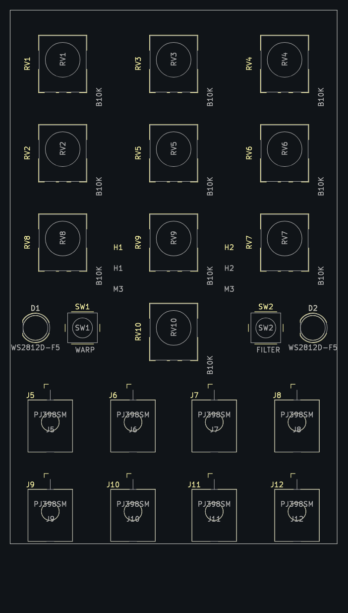
Only C1 and C2 (100 nF) and the two pin headers J3 and J4 (pin 1 at the top) go on the back. Everything else sits on the front: ten pots (RV1 TUNE … RV10 CUT CV), eight jacks (J5 V/OCT … J12 VOICE), two buttons, two LEDs.
Control board from the front. Caution: the orientation of the LEDs D1 and D2 on this silkscreen is wrong, see below.
Solder C1, C2 and the pin headers first.
Only insert the pots, jacks and buttons, put the printed front on and tighten the nuts lightly. Only then solder, so everything sits exactly in the holes.
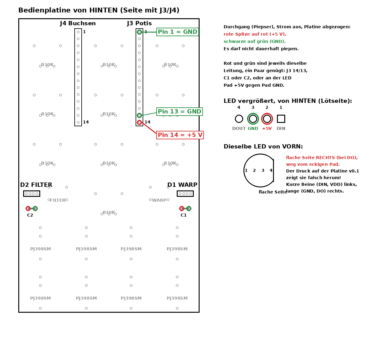
LEDs: do not follow the silkscreen. The v0.1 silkscreen shows the flat side at the square pad (pin 1), but on the WS2812D-F5 it is at DOUT (pin 4). Correct is:
The two shorter legs (DIN, VDD) into the square pad and the one next to it.
The two longer ones (GND, DOUT) on the other side.
Seen from the front, the flat side is on the right, away from the square pad.
Push them in far enough that the LEDs sit in the 5 mm holes with the front on, then solder.
The WS2812D-F5 from the front, as it should stand on the board.
The wrong way round, +5 V and ground reach the LED swapped; on the first build one burned out like that. If a pad tears off while desoldering: pad 4 (DOUT) of D2 is not connected, just cut the leg there.
Control board from the back (solder side): J3 pin 14 is +5 V, pins 1 and 13 are ground. There must be no permanent beep between +5 V and ground.
6. First check without chips
Do not put anything into the sockets yet; the DevKit and the DAC module stay out.
Visual check: solder bridges, forgotten joints, polarity of electrolytics and diodes.
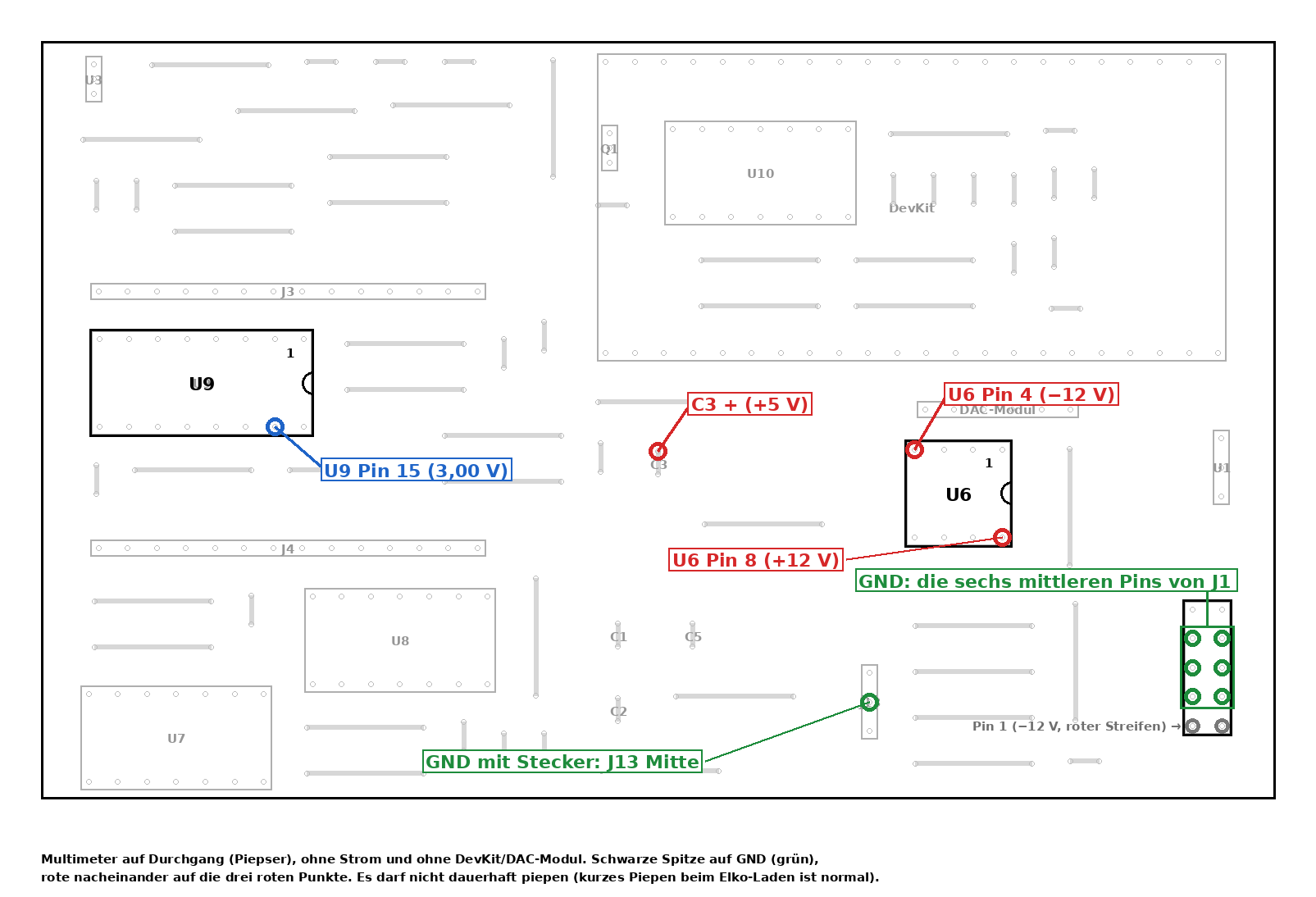
Multimeter on continuity, without power: +12 V, −12 V and +5 V must not be connected to ground (a short beep while the electrolytics charge is normal). Test points in the picture below.
Connect power, on a bench supply with a 50 mA limit per side, otherwise in the case (red stripe at pin 1 of J1 and on the bus at −12 V). The black probe on ground: the six middle pins of J1, or with the cable plugged in the middle pin of J13.
Where
Target
On the first build
U6 pin 8
about +11.7 V (+12 V minus a diode)
+11.8 V
U6 pin 4
about −11.7 V
−12.1 V
C3 + (5 V), also U10 pin 14
about +4.7 to 5 V
4.87 V
U9 pin 15 (reference)
3.00 V
3.01 V
There is no 3.3 V yet; it comes only with the DevKit, from its regulator.
If something is off or the current hits the limit: switch off and look for the fault before the chips go in.
Test points of the main board, component side, boxed header at the bottom right. Pin 1 of U9 is at the top right, pin 15 the second from the right in the bottom row.
7. Inserting chips and modules
Power off. Then insert, the notch as on the silkscreen:
U6 TL072, U7 and U8 MCP6004, U9 MCP3208, U10 74HCT125.
The DAC module onto its 6-pin header.
The DevKit onto its headers, USB towards the bottom edge (towards the side with the power connector).
Switch on again. Without firmware the LEDs show nothing (the small LED on the DevKit may blink; that is the manufacturer's test program); the current on +12 V should stay below about 150 mA.
In Chrome or Edge open Espressif's web flasher, baud rate 921600, Connect and select the DevKit. The DevKit has two USB sockets: use the one labelled “UART” (or “COM”).
Enter 0x0 as the flash address, choose the file, Program.
Under “Console” (115200 baud) you can then see what the module is doing.
On the first start the module computes its tables and stores them in flash, taking up to about a minute; meanwhile the LEDs light red and yellow and there is no sound. Every later start reads the tables in a fraction of a second. If both LEDs blink red, the PSRAM is missing (wrong DevKit).
Flashing works with and without Eurorack power; a diode separates the regulator from USB. New firmware is flashed the same way: the tables stay, but saved modes, hidden values and the V/Oct calibration are lost. So flash first, then calibrate.
Later updates also work without a cable over Wi-Fi, and they keep the settings and calibration: update over Wi-Fi. The first time (and from a firmware older than 1 November 2026) it has to be USB.
Building it yourself: ESP-IDF 5.3, idf.py build flash monitor in the firmware folder; the README on GitHub describes it.
9. Assembly and first sound
Fasten the control board to the front with the nuts of the pots and jacks, put the knobs on.
Plug the main board with its female headers onto the control board's pin headers and screw them together with the two standoffs (holes H1, H2).
Connect it in the case (red stripe at −12 V) and fix it to the rails with four M3 screws.
The VOICE output to a mixer. Without a cable in GATE the gate is permanently on; the module plays as a drone and should sound at once. Turn TUNE, TABLE and CUTOFF, press WARP and FILTER briefly: LED 1 and 2 change colour.
The outputs are at module level (±5 V), far too loud for headphones. How everything is operated: Operation.
10. Calibrating V/Oct
Switch off, only V/OCT plugged in, hold both buttons and switch on. LED 1 blinks white.
Exactly 1.000 V into V/OCT, press WARP. LED 2 blinks white.
Apply exactly 3.000 V, press FILTER.
Three times green: saved. Three times red: the values were implausible and the old ones stay; check voltage and cable and repeat.
Afterwards check with a tuner across several octaves.
Assembled variant (SMD)
Never built yet: the SMD boards are designed and checked (netlist against the parts list, design rules without errors), but never ordered, assembled or powered. Whoever orders them is the first. So far only the through-hole variant above has been built and heard.
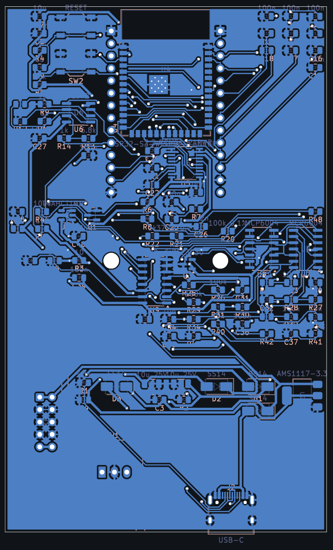
SMD main board from the back.
The same circuit, but the board manufacturer solders the main board: the ESP32-S3 module (WROOM-1 N16R8) directly on the board instead of the DevKit, the DAC as a chip instead of the module, all resistors, capacitors and chips in SMD on the back, plus a USB-C socket of its own for flashing and reset and boot buttons. Same dimensions, same front panel, same firmware; every control board fits every main board. The module is about 40 mm deep, 5 mm less than the through-hole variant.
Ordering
Order the main board (tonwerk-haupt) with assembly; the files are prepared for JLCPCB: upload the Gerber zip, turn on assembly, side Bottom (the parts sit on the back), then upload the bill of materials (BOM) and placement (CPL).
Before paying, look at the assembly preview: with packages such as SOT-223, SOT-23-5 and the SOICs on the bottom side, the rotation is often off by 90° or 180°; rotate them in the preview window then. Compare pin 1 of every chip with the dot on the silkscreen.
Replace parts that are out of stock with equivalent ones by value in the manufacturer's tool.
Control board: only C1/C2 on it are SMD, everything else is through-hole and by hand. It is simpler to order it unassembled, either tonwerk-bedien (C1, C2 as 0805 by hand) or straight away the through-hole tonwerk-bedien-tht from above.
Assembly costs considerably more than bare boards; a quote in October 2026 was about €180. In return almost all the soldering of the main board and the hunt for parts go away.
What is still soldered by hand
Main board: J1 (Eurorack connector, pin 1 = −12 V, red stripe), U1 (R-78E5.0-0.5), on the front the female headers J3 and J4 (1 × 14, pin 1 at the top, as in step 3, item 11), if you like the buttons SW1 (reset) and SW2 (boot).
The whole control board as in step 5, with the same warning about the LEDs: the LED silkscreen of the SMD control board v0.1 is the wrong way round too.
Checking, flashing, calibrating
Before the first power-up, check with the multimeter that +12 V, −12 V, +5 V and +3.3 V are not shorted to ground. Then power up with current limiting and measure: U6 pin 8 about +11.7 V, pin 4 about −11.7 V, the reference U3 3.00 V, plus 3.3 V at the regulator U2.
Flash through the main board's USB-C socket, with the same file at address 0x0 as in step 8. If the web flasher finds nothing: hold the boot button (solder in SW1 and SW2 for that), press reset briefly, release boot, then Connect once more. The module's messages come through the same socket.
Solder jumpers on the DAC module (step 4, especially 3 XSMT on H), the three wires to J13, is the TL072 the right way round? Listen at the DAC module's jack (headphones only quietly and not on your ears): if it sounds there, the fault lies between J13 and the output jacks (U6, R9–R14).
The filter acts on OSC instead of VOICE
L and R at J13 are swapped (step 4): L belongs on the square pad. Swap the two outer wires.
No sound on the first start
The tables are still being computed (step 8). Wait until the LEDs show the colours of the modes.
LEDs dark
U10 a 74HC125 instead of HCT? LEDs the right way round (step 5)? R48 (330 Ω) soldered?
An LED has burned out
It was the wrong way round (step 5). Desolder it and insert a new one the right way round.
LEDs in the wrong colours
Cyan shows as purple, magenta as turquoise, green as red: the ready-made images send red-green-blue, as the APA106 (and PL9823) expect, which are often sold as WS2812D-F5. Genuine Worldsemi WS2812D-F5s want green-red-blue: build the firmware yourself with idf.py -DTONWERK_LED_GRB=1 build flash.
Knobs do nothing or jump
A knob takes over only once it reaches the stored value (pick-up). Otherwise check the headers J3 and J4 and the 100 nF capacitors C10–C19.
CV inputs do nothing
MCP3208 (U9) and MCP6004 (U7, U8) the right way round? 3.0 V at U9 pin 15?
Console
Over USB (115200 baud) the module reports the load of the audio core every 5 seconds; errors at start-up appear there too.
As of 28 October 2026. The same guide is in the repository as BAUANLEITUNG.md (German). Boards, front panel, knobs and firmware are under the PolyForm Noncommercial License: building one for yourself yes, selling only with permission.